
 English


Varukorg
Din varukorg är tom, men det behöver den inte vara.
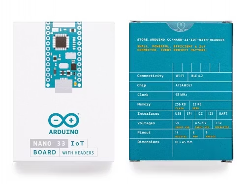
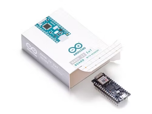
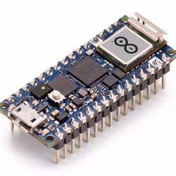
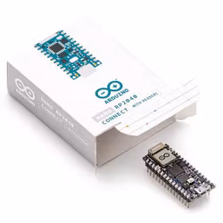
Lätt Användningen av en nano bord med tillägg av säker IoT och BT-anslutning.
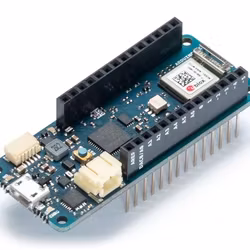
This small, robust and powerful board has WiFi and Bluetooth connectivity that combined with its low power architecture makes it a practical and cost-effective solution for your connected projects.
Arduino Nano 33 IoT is fully compatible with the Arduino IoT Cloud and supports full TLS secure transport: the ATECC608A cryptochip stores the cryptographic keys in hardware, offering a very high level of security for this class of products. The integration with the Arduino IoT Cloud offers also a very efficient way of setting up online dashboards with little coding and minimal effort.
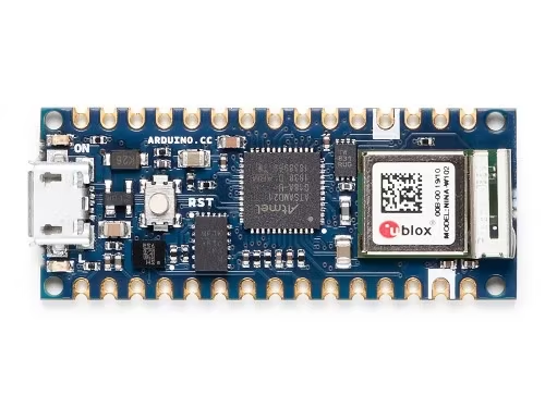
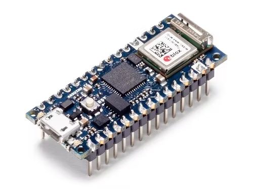
In the same iconic size of the Arduino Nano, the Arduino Nano 33 IoT hosts an Arm Cortex-M0+ SAMD21 processor, a WiFi and Bluetooth module based on ESP32, a 6 axis Inertial Measurement Unit (IMU) and a crypto chip which can securely store certificates and pre shared keys.
The board can either be used in a breadboard (when mounting pin headers), or as a SMT module, directly soldering it via the castellated pads.
With headers mounted.
In the Getting Started section, you can find all the information you need to configure your board, use the Arduino Software (IDE), and start to tinker with coding and electronics.
Do you want to learn more? Don’t miss the interview with Dario Pennisi, Arduino hardware and firmware development manager, who led the development of this board.
This board is based on the SAMD21G18A microcontroller.
| Clock | up to 48MHz |
| Flash | 256KB |
| SRAM | 32KB |
Please note: Arduino Nano 33 IoT only supports 3.3V I/Os and is NOT 5V tolerant so please make sure you are not directly connecting 5V signals to this board or it will be damaged. Also, as opposed to Arduino Nano boards that support 5V operation, the 5V pin does NOT supply voltage but is rather connected, through a jumper, to the USB power input.
To avoid such risk with existing projects, where you should be able to pull out a Nano and replace it with the new Nano 33 IoT, we have the 5V pin on the header, positioned between RST and A7 that is not connected as default factory setting. This means that if you have a design that takes 5V from that pin, it won’t work immediately, as a precaution we put in place to draw your attention to the 3.3V compliance on digital and analog inputs.
5V on that pin is available only when two conditions are met: you make a solder bridge on the two pads marked as VUSB and you power the NANO 33 IoT through the USB port. If you power the board from the VIN pin, you won’t get any regulated 5V and therefore even if you do the solder bridge, nothing will come out of that 5V pin. The 3.3V, on the other hand, is always available and supports enough current to drive your sensors. Please make your designs so that sensors and actuators are driven with 3.3V and work with 3.3V digital IO levels. 5V is now an option for many modules and 3.3V is becoming the standard voltage for electronic ICs.
The communication on WiFi and Bluetooth is managed by a NINA W102 ESP32 based module. The module is connected to the SAMD21 microcontoller with an SPI BUS and a serial port through the following pins:
| SAMD21 Pin | SAMD21 Acronym | NINA Pin | NINA Acronym | Description |
| 13 | PA8 | 19 | RESET_N | Reset |
| 39 | PA27 | 27 | GPIO0 | Attention Request |
| 41 | PA28 | 7 | GPIO33 | Acknowledge |
| 23 | PA14 | 28 / 21 | GPIO5 / GPIO19 | SPI CS / UART RTS |
| 24 | PA15 | 29 / 20 | GPIO18 / GPIO22 | SPI CLK / UART CTS |
| 22 | PA13 | 1 | GPIO21 | SPI MISO |
| 21 | PA12 | 36 | GPIO12 | SPI MOSI |
| 31 | PA22 | 23 | GPIO3 | Processor TX -> Nina RX |
| 32 | PA23 | 22 | GPIO1 | NINA TX -> Processor RX |
Some of the NINA W102 pins are connected to the 15+15 pins headers/pads and can be directly driven by the module's ESP32; in this case it is necessary that the SAMD21 corresponding pins are aptly tri-stated. Below is a list of such signals:
| SAMD21 Pin | SAMD21 Acronym | NINA Pin | NINA Acronym | Header Description |
| 48 | PB03 | 8 | RESET_N | A7 |
| 14 | PA09 | 5 | GPIO0 | A6 |
| 8 | PB09 | 31 | GPIO33 | A5/SCL |
| 7 | PB08 | 35 | GPIO5 / GPIO19 | A4/SDA |
The IMU is a LSM6DSL and it is managed through I2C.
The crypto chip is an ATECC608A and has a supporting library that is used by the WiFiNINA library.
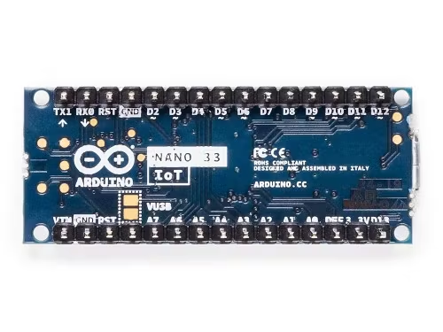
The board has a two 15 pins connectors - one on each side -, pin to pin compatible with the original Arduino Nano.
| Pin | Funcion | Type | Description |
| 1 | D13 | Digital | GPIO |
| 2 | +3V3 | Power Out | Internally generated power output to external devices |
| 3 | AREF | Analog | Analog Reference; can be used as GPIO |
| 4 | A0/DAC0 | Analog | ADC in/DAC out; can be used as GPIO |
| 5 | A1 | Analog | ADC in; can be used as GPIO |
| 6 | A2 | Analog | ADC in; can be used as GPIO |
| 7 | A3 | Analog | ADC in; can be used as GPIO |
| 8 | A4/SDA | Analog | ADC in; I2C SDA; Can be used as GPIO (*) |
| 9 | A5/SCL | Analog | ADC in; I2C SCL; Can be used as GPIO(*) |
| 10 | A6 | Analog | ADC in; can be used as GPIO |
| 11 | A7 | Analog | ADC in; can be used as GPIO |
| 12 | VUSB | Power In/Out | Normally NC; can be connected to VUSB pin of the USB connector by shorting a jumper |
| 13 | RST | Digital In | Active low reset input (duplicate of pin 18) |
| 14 | GND | Power | Power Ground |
| 15 | VIN | Power In | Vin Power input |
| 16 | TX | Digital | USART TX; can be used as GPIO |
| 17 | RX | Digital | USART RX; can be used as GPIO |
| 18 | RST | Digital | Active low reset input (duplicate of pin 13) |
| 19 | GND | Power | Power Ground |
| 20 | D2 | Digital | GPIO |
| 21 | D3/PWM | Digital | GPIO; can be used as PWM |
| 22 | D4 | Digital | GPIO |
| 23 | D5/PWM | Digital | GPIO; can be used as PWM |
| 24 | D6/PWM | Digital | GPIO; can be used as PWM |
| 25 | D7 | Digital | GPIO |
| 26 | D8 | Digital | GPIO |
| 27 | D9/PWM | Digital | GPIO; can be used as PWM |
| 28 | D10/PWM | Digital | GPIO; can be used as PWM |
| 29 | D11/MOSI | Digital | SPI MOSI; can be used as GPIO |
| 30 | D12/MISO | Digital | SPI MISO; can be used as GPIO |
(*) As opposed to other Arduino Nano boards, pins A4 and A5 have an internal pull up and default to be used as an I2C Bus so usage as analog inputs is not recommended. Opposed to Arduino Nano boards that support 5V operation, the 5V pin does NOT supply voltage but is rather connected, through a jumper, to the USB power input.
On the bottom side of the board, under the communication module, debug signals are arranged as 3x2 test pads with 100 mil pitch. Pin 1 is the bottom left one with the USB connector on the left and the test pads on the right
| Pin | Function | Type | Description |
| 1 | +3V3 | Power Out | Internally generated power output to be used as voltage reference |
| 2 | SWD | Digital | SAMD11 Single Wire Debug Data |
| 3 | SWCLK | Digital In | SAMD11 Single Wire Debug Clock |
| 4 | UPDI | Digital | ATMega4809 update interface |
| 5 | GND | Power | Power Ground |
| 6 | RST | Digital In | Active low reset input |


Din varukorg är tom, men det behöver den inte vara.