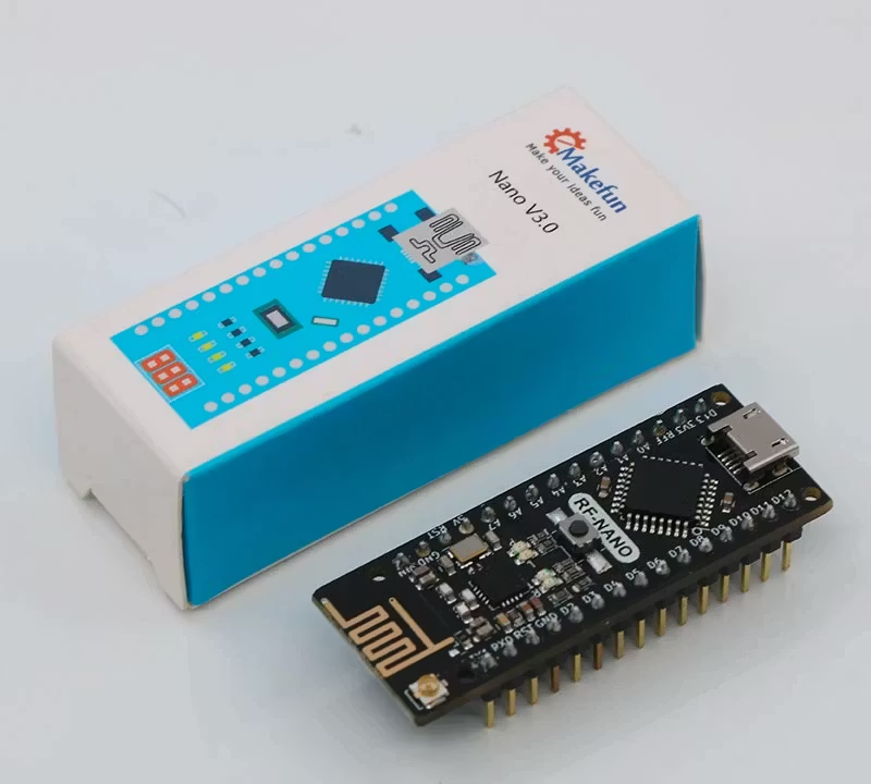
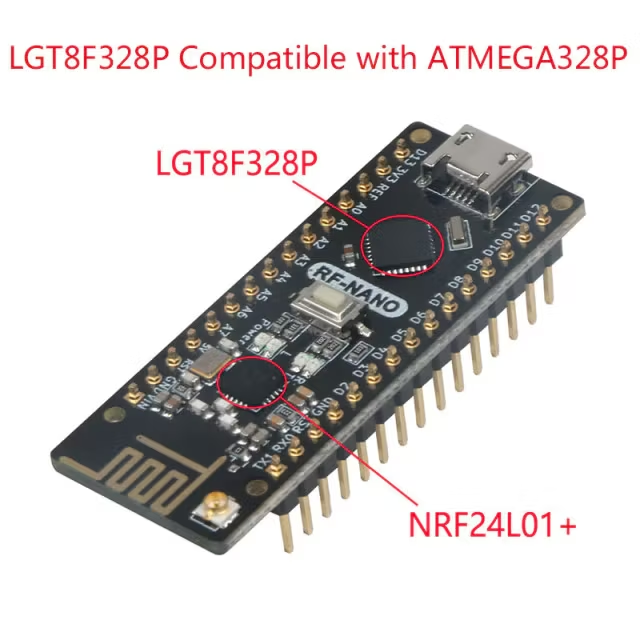
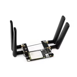
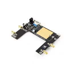
Emakefun LGT-RF-Nano for Arduino Nano V3.0 RF-NANO LGT8F328P Integrate NRF24l01+ Micro USB Nano Board with Antenna Interface.
Main Feature
1. Creative product LGT-RF-Nano Board: compatible with arduino nano v3.0, integrated LGT8F328P and nrf24l01+, with software package support, more convenient to use.
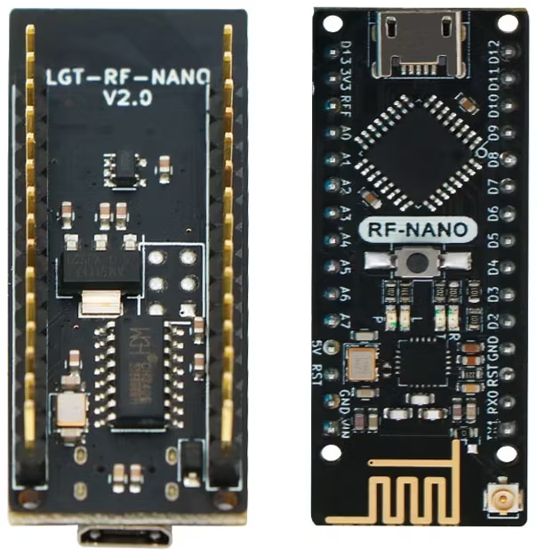
2. Ultra-small size design, smooth and beautiful appearance: PCB size is only 48mm*19mm, and the pins are fully compatible with Nano V3.0, no soldering is required. The micro usb interface is more convenient to use.
3. The price is more advantageous, compatible with atmega328p-rf-nano, both can achieve the same function, but the price of LGT-RF-Nano is very favorable.
4. Professional technical team support and perfect information website, you can contact us at any time if you have any questions.
LGT-RF-NANO information website:
LGT-RF-NANO information och codes
Specification:
Microcontroller LGT8F328P
Nrf24L01+ 2.4G wireless
Architecture AVR
Operating Voltage 5 V
Flash Memory 32 KB of which 2 KB used by bootloader
SRAM 2 KB
Clock Speed 16 MHz
Analog I/O Pins 8
EEPROM 1 KB
DC Current per I/O Pins 40 mA (I/O Pins)
Input Voltage 7-12 V
Digital I/O Pins 22
PWM Output 6
Power Consumption 19 mA
PCB Size 48 x 18mm
Weight 8g
What is the LGT8F328P ?
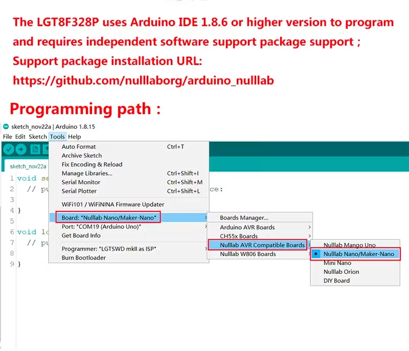
The LGT8F328P is a chip compatible with AVR instruction set and Atmega328P. After loading the Arduino software support package, you can use the Arduino IDE to program. The usage method and 99.9% of the application scenarios can replace the Atmega328P chip.
LGT8F328P Parameter:
1. The LGT8F328P enhances 8-bit RISC core, supports 16-bit digital operation expansion, and can run at a core frequency of up to 32MHz within the working range of 1.8V-5.5V;
2. The LGT8F328P internal 32K bytes of FLASH program memory, 2K bytes of data SRAM, built-in control logic that simulates FLASH as EEPROM, part of the program FLASH can be divided into data FLASH space according to application needs, and EEPROM-like interface access is realized through the EEPROM controller ;
3. The LGT8F328P integrates a wealth of analog peripherals, including 12-bit ADC, programmable gain differential amplifier, high-precision 1.024/2.048/4.096V internal reference voltage, 8-bit DAC and high-speed analog comparator; at the same time LGT8F328P also integrates commonly used digital Interface controller, supports multi-channel complementary PWM output and dead zone control;
4. The LGT8F328P architecture design is relatively new, and its peripheral functions are far stronger than that of the Atmega328P. In particular, the program encryption capability far exceeds Atmega328P.
Why use LGT8F328P instead of Atmega328P?
As we all know, the shortage of chips will also have a great impact on the maker industry. The price of Atmega328P chips has already doubled and the supply is unstable. The market is full of refurbished, copycats, and even typing (printed on the same package) chips, which seriously interferes with the normal production and use of Maker's products. I came into contact with the LGT8F328P chip by chance. At first, I thought it was a fake chip. After rigorous testing and direct communication with the chip manufacturer, I found that it was an AVR instruction set chip, not a fake chip. Similar to GD to STM32. It is a brand-new chip, but it is compatible to replace Atmega328P. After testing and optimization by the Nulllab technical team for more than half a year, our arduino IDE software support package is 99.9% compatible with Atmega328P. In this way, makers can buy cost-effective and reliable arduino products. The Nulllab technical team provides long-term technical support and chip supply for this, so makers can use it with confidence.

 Svenska
